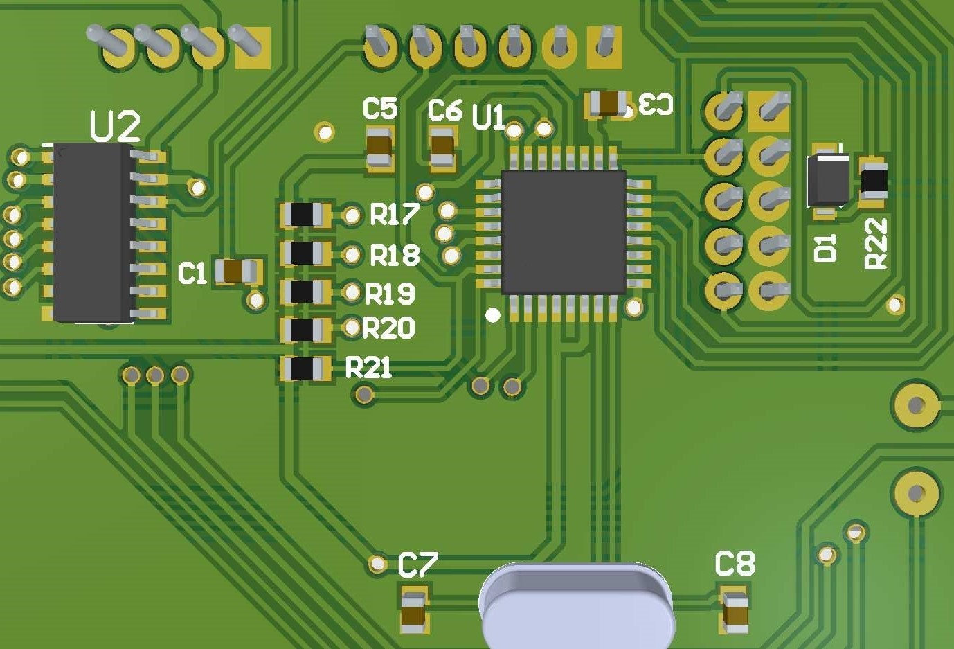
PCB Layout Design
Designing the layout of your printed circuit board is crucial to creating a reliable, cost-effective board. While circuit design and component selection are also essential, you should always make sure you leave enough time for PCB layout. A lot goes into determining the optimal PCB layout design, especially since today’s boards are becoming more complex, compact and lightweight. Typically, PCB design falls under the Hardware (HW) design category of engineering. It ties in electrical, mechanical, software, systems, test, and manufacturing disciplines to include electrical (ECAD) and mechanical (MCAD) designers. PCB DESIGN STEPS- 1.Concept-First and foremost functioning has to get finalized because it determines what king of pcb will be designed and fabricated , even if a pcb is needed or not if yes what kind of signals will be travelling through it. 2.Schematic-Next step is to get the hand drawn circuit to be rebuilt but now in a CAD software which has this kind of capability to make schematics. 3.Component Placement- Then the selected components are placed on the board virtually with keeping many constraints in mind to get the desired output and putting connectors,sensors etc where they should be putted so that anyone can use them to give an input or take output. 4.Routing- After component placement is fixed routing is done between the componenets so when pcb is fabricated it will have copper traces between them ,which will electrically connect the components togethor.